Tower Optical: Revolutionizing Photonics with Expanded Capabilities
Wednesday, 4 February, 2026Large Waveplates: Tower Optical’s Breakthrough for High-Energy Lasers
Sunday, 8 February, 2026Introduction: A New Manufacturing Threshold
Scaling in advanced manufacturing is never trivial. It demands rigor, capital discipline, and a deep understanding of materials science. The ability to produce silicon wafers up to the 10-inch class marks a consequential inflection point—one that reshapes cost structures, expands application scope, and signals technical maturity. This development reflects a deliberate ascent rather than a hurried leap.
About Tower Optical Corporation
Legacy of Precision Optics
Tower Optical Corporation has long operated at the confluence of craftsmanship and engineering. Its reputation has been built on exacting tolerances, disciplined process control, and an unwavering focus on optical performance. Over time, those competencies have translated naturally into adjacent domains where surface perfection and dimensional fidelity are paramount.
Evolution Toward Advanced Substrates
The move into larger-diameter silicon substrates is an evolutionary step. It leverages institutional knowledge in polishing science, metrology, and contamination control—capabilities that become exponentially more critical as wafer diameters increase.
Understanding Silicon Wafer Scaling
Why Diameter Matters
Wafer diameter is not a vanity metric. Larger formats increase usable area per run, reduce per-die cost, and align production with contemporary toolsets. Each incremental inch compounds complexity, demanding tighter control over bow, warp, and micro-topography.
From Small Formats to 10-Inch Class
Transitioning to 10-inch wafers requires recalibration across the production stack. Equipment envelopes expand. Thermal gradients must be managed. Process windows narrow. Mastery here is a marker of operational sophistication.
What “Up to 10 Inch” Production Enables
Yield Economics and Throughput
With larger wafers, manufacturers can extract more functional area from a single process cycle. The economics improve quietly but decisively. Throughput rises. Scrap rates, when properly managed, fall in relative terms.
Platform Compatibility Across Tools
Many modern fabrication and research tools are optimized for larger wafer standards. Producing up to 10 inches ensures compatibility, reduces handling adaptations, and simplifies integration into existing workflows.
Manufacturing Capabilities Behind the Milestone
Crystal Growth and Slicing
The journey begins upstream. High-purity silicon must be grown with crystalline uniformity, then sliced with minimal subsurface damage. Blade selection, feed rates, and coolant chemistries all matter—immensely.
Lapping, Polishing, and Flatness Control
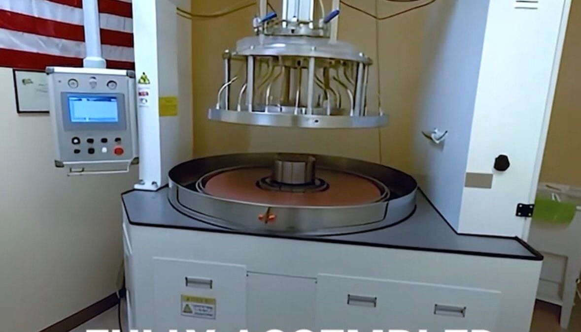
Achieving optical-grade surfaces at this scale is exacting. Multi-stage lapping removes deformation. Polishing refines roughness to near-atomic smoothness. Flatness is measured not in millimeters, but in microns—and sometimes less.
Quality, Metrology, and Process Control
Surface Integrity and Defect Density
As diameter increases, so does the probability of defects. Controlling particles, scratches, and crystallographic anomalies requires immaculate environments and disciplined protocols.
Inline Inspection and Feedback Loops
Modern production relies on continuous measurement. Interferometry, surface profilometry, and automated inspection feed data back into the process, allowing rapid correction before deviations propagate.
Applications Unlocked by Larger Wafers
Photonics and Precision Optics
Larger silicon wafers support advanced photonic architectures, enabling integrated optical components with greater consistency and alignment accuracy. For optics, uniformity across a broader aperture is invaluable.
Semiconductor R&D and Specialty Devices
Research environments benefit from scale without sacrificing customization. Specialty devices, pilot runs, and experimental architectures all gain from access to larger, high-quality substrates.
Supply Chain and Customer Impact
Lead Times, Consistency, and Customization
Expanded capability often translates to steadier supply. Customers can expect improved consistency across batches, alongside options for tailored specifications that reflect unique performance requirements.
Domestic Capability and Resilience
Local production of large-diameter wafers reduces logistical friction. It also enhances resilience in an era where supply chains are scrutinized as closely as balance sheets.
Industry Implications
Competitive Positioning
Producing up to 10-inch silicon wafers places Tower Optical Corporation in rarified company. It signals readiness to serve demanding markets where scale and precision are non-negotiable.
Innovation Velocity
With scale comes speed. Development cycles compress. Iteration accelerates. Innovation becomes less constrained by material availability and more driven by imagination.
Looking Ahead
Roadmap Considerations
Reaching 10 inches is not an endpoint. It is a platform. Future refinements—thinner wafers, tighter tolerances, novel finishes—remain within reach.
Continuous Improvement Ethos
Manufacturing excellence is cumulative. Each advancement builds on the last, guided by data, discipline, and an unrelenting pursuit of better outcomes. The capacity to produce silicon wafers up to 10 inches stands as a testament to that philosophy.


